PCB 주문을 할때 비용 절감을 위해서 PCB 기판에 같은 보드를 여러개 동시에 배치하는 것을 미쿡에서는 Panelizing이라고 한다.
전에 PCB Layout 시간에도 다루었지만 Seeed Studio에서도 서브 보드를 5개까지 허용한다. 대신 너무 아쉬운 점은 자르는 것은 각자의 몫이라는 것이다. PCB를 자를수 있는 밴드 쏘우를 또 구해야 할 판이다. 비용 좀 더 받고 잘라 주면 좋을 텐데...
하여튼 Eagle CAD Light 버전에는 복사기능이 막혀 있어, 이 작업을 도와주는 GerbMerge 라는 프로그램이 있다. 이게 Python 어플이라 먼저 아래와 같은 어플이 설치가 되어 있어야 한다.
- Python version 2.4 or later
- SimpleParse version 2.1.0 or later
Python 은 3.x 도 있는데 혹시 몰라서 2.7 버전을 설치했다.
Seeed Studio는 전체 패널의 아웃라인을 요구해서 GerbMerge 를 패치할 필요가 있단다. gerberge-patched github repo 여기서 zip 파일을 다운받아서 gerbmerge 폴더를 C:\Python<version>\Lib\site-packages\gerbmerge (윈도우일 경우) 폴더에 덮어 쓴다. 전에 작업한 FT232-Breakout 보드를 merge 해 볼 것이다. CAM 작업으로 생성한 7개파일을 C:\Python<version>\FT232-Breakout-v10 폴더를 만들어 복사해 온다.
<board>.GTO - top silkscreen
<board>.GTS - top soldermask
<board>.GTL - top copper
<board>.GBO - bottom silkscreen
<board>.GBS - bottom soldermask
<board>.GBL - bottom copper
<board>.TXT - Excellon drill file.
그리고 config 파일과, layout 파일을 만든다.
panel.cfg 파일내용
#------------------------------------------------------------------------------------------------------------
[DEFAULT]
# I always use the local directory to contain all input gerbers, config files, and output files
projdir = FT232-Breakout-v10
# MergeOut is the prefix of the output files.
MergeOut = merge2
[Options]
# CutlineLayers will determine where the subboard markings are, which will help in separating them. These are the accentuated lines between the two instances of the board in the image below.
CutLineLayers = *topsilkscreen,*bottomsilkscreen
CropMarkLayers = *topsilkscreen,*bottomsilkscreen
# OutlineLayers is used by the patched gerbmerge, it defines which layers the entire panel outline will be drawn on. Seeed requires this on all layers.
OutlineLayers = *toplayer,*bottomlayer,*topsilkscreen,*bottomsilkscreen,*topsoldermask,*bottomsoldermask
FabricationDrawingFile = %(mergeout)s.fab
ExcellonLeadingZeros = 0
OutlineLayerFile = %(mergeout)s.oln
ScoringFile = %(mergeout)s.sco
# here you can specify the maximum dimensions allowed by the Seeed PCB service you ordered (in inches).
# gerbmerge will warn you if your final panel (based on your layout) exceeds these dimensions.
PanelWidth = 3.93
PanelHeight = 1.965
# comment out the margins or set them to zero if you want the maximum amount of useable area on your panel.
#LeftMargin = 0.1
#RightMargin = 0.1
#TopMargin = 0.1
#BottomMargin = 0.1
# spacing determines how much space between the panels. I found 0.0625 to be plenty of space for a band-saw blade, I may reduce it a hair in the next run.
XSpacing = 0.0625
YSpacing = 0.0625
CutLineWidth = 0.01
CropMarkWidth = 0.01
AllowMissingLayers = 1
DrillClusterTolerance = 0.002
MinimumFeatureSize = *topsilkscreen,0.008,*bottomsilkscreen,0.008
# if you define the merge output files to be in the filename scheme that Seeed requires, you won't have to rename them by hand later.
[MergeOutputFiles]
Prefix = %(mergeout)s
*TopLayer=%(prefix)s.GTL
*BottomLayer=%(prefix)s.GBL
*TopSilkscreen=%(prefix)s.GTO
*BottomSilkscreen=%(prefix)s.GBO
*TopSoldermask=%(prefix)s.GTS
*BottomSoldermask=%(prefix)s.GBS
Drills=%(prefix)s.TXT
BoardOutline=%(prefix)s.bor
ToolList = toollist.%(prefix)s.drl
Placement = placement.%(prefix)s.txt
# Job configuration - for each different sub-board, define a section like follows with the subboard name (used in the layout file) and the gerbers comprising that job.
[FT232-Breakout-v10]
Prefix=%(projdir)s/FT232-Breakout-v10
# List all the layers that participate in this job. Required layers are Drills
# and BoardOutline and have no '*' at the beginning. Optional layers have
# names chosen by you and begin with '*'. You should choose consistent layer
# names across all jobs.
*TopLayer=%(prefix)s.GTL
*BottomLayer=%(prefix)s.GBL
*TopSilkscreen=%(prefix)s.GTO
*BottomSilkscreen=%(prefix)s.GBO
*TopSoldermask=%(prefix)s.GTS
*BottomSoldermask=%(prefix)s.GBS
Drills=%(prefix)s.TXT
BoardOutline=%(prefix)s.BOR
#-----------------------------------------------------------------------------------------------------------------
panel.layout 파일내용
칼럼 추가시 콤마없이 엔터치고 추가하면 된다.
#-----------------------------------------------------------------------------------------------------------------
Row {
Col {
FT232-Breakout-v10
}
Col {
FT232-Breakout-v10
}
}
10cm x 5cm 크기에 merge 한다고 가정하고 작업을 했다. 근데 여기서 헤맨 부분은 bor 파일이 필요한데
Seeed_Gerber_Generater_v0r95_DrillAlign.cam 파일로 gerber 파일을 생성해 봐도 bor 파일은 없다는 거다. 그런데 이 파일이 보드 아웃라인 파일이여서 GBO 파일이 아웃라인만 나타내므로 이걸 복사해서 bor 파일로 만들어서 작업해보니 merge가 되었다. 아래와 같이 실행하면 된다.
C:\Python<version>>python.exe C:\Python<version>\Lib\site-packages\gerbmerge\gerbmerge.py panel.cfg panel.layout
layout이 잘못 설정되면 패널 사이즈를 초과했다는 메세지를 표시한다.

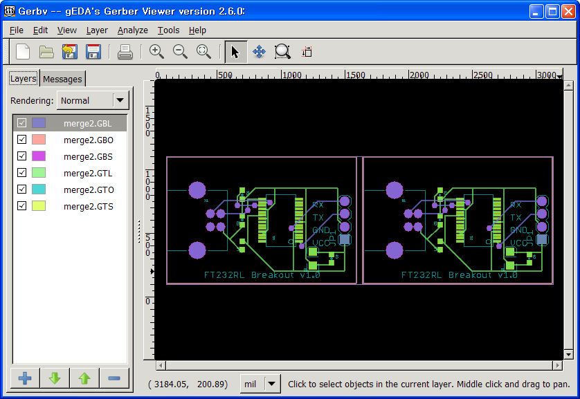
정상적으로 merge가 되면 아래와 같이 나타난다.
Windows 7 운영체제에서는 설치파일은 관리자권한으로 설치하고 cmd.exe 파일도 관리자권한으로 실행해야 에러가 나지 않는다.


Seeed Studio는 전체 패널의 아웃라인을 요구해서 GerbMerge 를 패치할 필요가 있단다. gerberge-patched github repo 여기서 zip 파일을 다운받아서 gerbmerge 폴더를 C:\Python<version>\Lib\site-packages\gerbmerge (윈도우일 경우) 폴더에 덮어 쓴다. 전에 작업한 FT232-Breakout 보드를 merge 해 볼 것이다. CAM 작업으로 생성한 7개파일을 C:\Python<version>\FT232-Breakout-v10 폴더를 만들어 복사해 온다.
<board>.GTO - top silkscreen
<board>.GTS - top soldermask
<board>.GTL - top copper
<board>.GBO - bottom silkscreen
<board>.GBS - bottom soldermask
<board>.GBL - bottom copper
<board>.TXT - Excellon drill file.
그리고 config 파일과, layout 파일을 만든다.
panel.cfg 파일내용
#------------------------------------------------------------------------------------------------------------
[DEFAULT]
# I always use the local directory to contain all input gerbers, config files, and output files
projdir = FT232-Breakout-v10
# MergeOut is the prefix of the output files.
MergeOut = merge2
[Options]
# CutlineLayers will determine where the subboard markings are, which will help in separating them. These are the accentuated lines between the two instances of the board in the image below.
CutLineLayers = *topsilkscreen,*bottomsilkscreen
CropMarkLayers = *topsilkscreen,*bottomsilkscreen
# OutlineLayers is used by the patched gerbmerge, it defines which layers the entire panel outline will be drawn on. Seeed requires this on all layers.
OutlineLayers = *toplayer,*bottomlayer,*topsilkscreen,*bottomsilkscreen,*topsoldermask,*bottomsoldermask
FabricationDrawingFile = %(mergeout)s.fab
ExcellonLeadingZeros = 0
OutlineLayerFile = %(mergeout)s.oln
ScoringFile = %(mergeout)s.sco
# here you can specify the maximum dimensions allowed by the Seeed PCB service you ordered (in inches).
# gerbmerge will warn you if your final panel (based on your layout) exceeds these dimensions.
PanelWidth = 3.93
PanelHeight = 1.965
# comment out the margins or set them to zero if you want the maximum amount of useable area on your panel.
#LeftMargin = 0.1
#RightMargin = 0.1
#TopMargin = 0.1
#BottomMargin = 0.1
# spacing determines how much space between the panels. I found 0.0625 to be plenty of space for a band-saw blade, I may reduce it a hair in the next run.
XSpacing = 0.0625
YSpacing = 0.0625
CutLineWidth = 0.01
CropMarkWidth = 0.01
AllowMissingLayers = 1
DrillClusterTolerance = 0.002
MinimumFeatureSize = *topsilkscreen,0.008,*bottomsilkscreen,0.008
# if you define the merge output files to be in the filename scheme that Seeed requires, you won't have to rename them by hand later.
[MergeOutputFiles]
Prefix = %(mergeout)s
*TopLayer=%(prefix)s.GTL
*BottomLayer=%(prefix)s.GBL
*TopSilkscreen=%(prefix)s.GTO
*BottomSilkscreen=%(prefix)s.GBO
*TopSoldermask=%(prefix)s.GTS
*BottomSoldermask=%(prefix)s.GBS
Drills=%(prefix)s.TXT
BoardOutline=%(prefix)s.bor
ToolList = toollist.%(prefix)s.drl
Placement = placement.%(prefix)s.txt
# Job configuration - for each different sub-board, define a section like follows with the subboard name (used in the layout file) and the gerbers comprising that job.
[FT232-Breakout-v10]
Prefix=%(projdir)s/FT232-Breakout-v10
# List all the layers that participate in this job. Required layers are Drills
# and BoardOutline and have no '*' at the beginning. Optional layers have
# names chosen by you and begin with '*'. You should choose consistent layer
# names across all jobs.
*TopLayer=%(prefix)s.GTL
*BottomLayer=%(prefix)s.GBL
*TopSilkscreen=%(prefix)s.GTO
*BottomSilkscreen=%(prefix)s.GBO
*TopSoldermask=%(prefix)s.GTS
*BottomSoldermask=%(prefix)s.GBS
Drills=%(prefix)s.TXT
BoardOutline=%(prefix)s.BOR
#-----------------------------------------------------------------------------------------------------------------
panel.layout 파일내용
칼럼 추가시 콤마없이 엔터치고 추가하면 된다.
#-----------------------------------------------------------------------------------------------------------------
Row {
Col {
FT232-Breakout-v10
}
Col {
FT232-Breakout-v10
}
}
#-----------------------------------------------------------------------------------------------------------------
10cm x 5cm 크기에 merge 한다고 가정하고 작업을 했다. 근데 여기서 헤맨 부분은 bor 파일이 필요한데
Seeed_Gerber_Generater_v0r95_DrillAlign.cam 파일로 gerber 파일을 생성해 봐도 bor 파일은 없다는 거다. 그런데 이 파일이 보드 아웃라인 파일이여서 GBO 파일이 아웃라인만 나타내므로 이걸 복사해서 bor 파일로 만들어서 작업해보니 merge가 되었다. 아래와 같이 실행하면 된다.
C:\Python<version>>python.exe C:\Python<version>\Lib\site-packages\gerbmerge\gerbmerge.py panel.cfg panel.layout
layout이 잘못 설정되면 패널 사이즈를 초과했다는 메세지를 표시한다.

Windows 7 운영체제에서는 설치파일은 관리자권한으로 설치하고 cmd.exe 파일도 관리자권한으로 실행해야 에러가 나지 않는다.

생성된 파일을 Gerbv로 열어서 확인해 봤다.
이상이 없으면 Seeed Studio의 Fusion PCB Service에 신청하면 될 것 같다.
댓글 없음:
댓글 쓰기